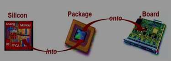
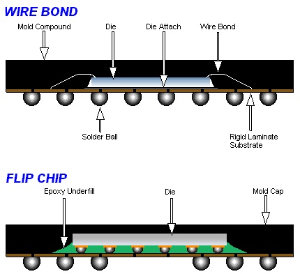
“Flip Chip” describes the method used to connect a semiconductor die to a substrate: The dies are bumped and then “flipped” onto a substrate.
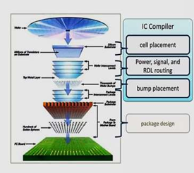
- This application note describes the die-driven flow with a peripheral ring I/O style.
- As silicon processes migrate to 45nm and below, flip- chip designs are becoming more prevalent,
- In flip-chip design style, there are no bonding wires.
- It increases the number of I/O and improve timing between I/O and core logic.
- Flip-chip design requires a more sophisticated design methodology.
Package substrate:
- PGA(pin grid array)
- BGA(ball grid array
Two technique to mount the die to the substrate:
- 1.Wire bonding ,WB.
- Flip chip, FC
Benefits
- High pin count
- High signal density
- Better power dissipation
- Low signal inductance, and good power/ground connectivity.
- Ideal for high-speed interfaces (including RF) that wire bonds cannot support
- Good Assembly dynamics
Traditional
–Wireless and Communications
- Shorter path from die to the substrate
– Space consideration applications
- Handheld/ bodyworn, etc
Today’s Applications
– Automotive
- Military/Aerospace
– Computing
- Life Sciences
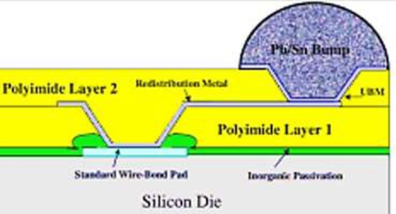
Bump on Pad & RDL:
Wafer Bumping can be considered as a step in wafer processing where solder spheres are attached to the I/O pads.
- Some wafers are designed to be flip chips and bumps go directly on pads.
- A Redistribution layer (RDL) is added to a wirebond die to establish bumps that are compatible with the assembly of a die on a Printed Circuit board
- Paste-printed bumps, plated bumps, or placed preformed solder spheres are typically mounted onto a fluxed, under bump metallization (UBM) material, that is plated or sputtered onto the die pads (Al or Cu), to insure good adhesion of the bumps.
- Wafer bump compositions: gold, eutectic, lead tin, lead free, high lead materials, or Cu pillar. The bump size and bump pitch may vary depending on pad count, signal integrity, and assembly design rules.
PACKAGING TECHNOLOGY:
Integrated circuits are put into protective packages to allow easy handling and assembly onto printed circuit boards and to protect the device from damage.
WIRE BONDING:
This conventional technique involves the mounting of a chip onto a substrate, back-side down. Then, peripheral pads on the chip are bonded to the substrate via wires. The main advantage of this approach is that it is cost-effective.
PACKAGING EXAMPLES:
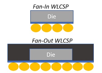
WLCSP – Wafer Level Chip Scale Package – NO Substrate
- FAN-IN
- Wafer Level Chip Scale Package (WLCSP) is a die- sized package with bumps that are essentially balls that can be soldered directly to a PCB.
- Bump on Pad (BOP): Solder bumps attached directly to the die pad openings, that gives the shortest path from die circuit to PCB, so achieves optimum signal performance, lowest inductance, highest speed).
FAN-OUT
- eWLB is similar to the WLCSP, however the wafers are first diced, the dies spaced apart on tape & frame, and a resin material is flowed over the dies then hardened to form a re-constituted wafer.
- Referred to as “Fan Out” because the relatively small pitch die pads are able to be routed out (fanned out) to a larger pitch array of balls over the peripheral epoxy resin.
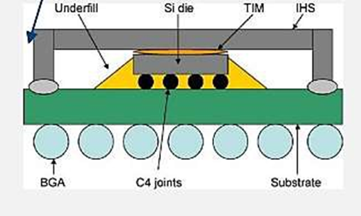
FCBGA – Flip Chip Ball Grid Array
- Flip Chip BGA packages: Still the most common package for bumped dies.
Advantages:
- Good thermal performance, and scalability for large and complex dies.
- Low cost FCBGAs use a laminate (PCB type) substrate.
- Build-up substrates are also an option, offering –
- Finer pitch routing, enhanced signal and thermal performance, and a lower profile, at a cost.
- FCBGA is the preferred flip chip solution for high power designs and designs with a large number of balls (over 100, for example).
Contact Us: info@sysargus.com
Learning Platform for Product Engineering professionals imparting guidance and sharing knowledge on Electronics System Design Best Practices.
Connect with us:-