What is Panelization?
PCB panelization is a fabrication technique that allows smaller PCBs to be produced and joined together as a single array, making it easier to run through the assembly line. It is also simple to depanelize or remove each board from the array for shipping or product installation.
Alternatively, a PCB processing edge around an individual PCB can be used to increase the width to fit on the assembly line.
If you want to take advantage of the benefits of mass production that come with Panelization, there are a few things to consider. The details are as follows:
Component layout: Panelization options for components and connectors, particularly those hanging off the edge of a PCB, may be limited by component arrangement. As a result, sensitive SMT (surface mount technology) components should be placed toward the edge of a PCB.
Tooling holes: Room for tooling holes on the processing edges of arrays and break-away can be provided so that automated testing can be performed on the assembly line.
PCB shape: The shape of your PCB can make Panelization more difficult. If your PCB geometry is complex, alternating images from 90° to 180° can make a big difference in terms of optimizing space on a panel. With a CAD application, it can also fit strangely shaped PCBs into an array.
PCB-array strength: There is a trade-off between array integrity and ease of depanelization during production. Increasing the board count for each array can improve strength and reduce vibration.
Panelization aspects
There are several penalization methods available, each with its own set of advantages and disadvantages. The design of the boards on the panel, as well as the panel itself, will often determine which penalization approach is appropriate for the job. The following are the most notable of these factors:
Design: The most important factor in identifying the most effective panelization technology is the board design. Certain methods may be less suitable than others due to the amount of clearance between components and the board’s edge, as well as the presence of edge-hanging components.
Components: The type of components utilized on the board is just as significant as where they are placed. The most appropriate breakout and penalization strategy may be influenced by particularly sensitive components and connectors.
Materials: Because some materials are more prone to splintering during the breakout process, the materials used in a PCB may limit the type of penalization approach that is most appropriate. Board thickness is also important, as thin boards are more likely to break during assembly, whereas thick boards are more difficult to break during the breakout process.
The following are some of the penalization methods.
V-score penalization:
Unique V-shape PCBs are distinguished from one another using this common paneling technique. With an angled blade from the two ends of the board, top, and bottom, these ruts remove nearly a third of the thickness of the board. Given the surprisingly strong remains of the third portion between both grooves and the strain on the PCB and its nearby components by hand, a machine is used to complete the break-out process.
Solid Tab Panelization:
With strong tabs throughout each board, modules can be added to boost present efficacy. However, a CNC router, a laser slicing machine, and a blade tool in the form of a hook are required for this type of panel removal. The router may produce dust and vibration, while the laser cutter on panels thicker than 1 mm is extremely expensive and inefficient. The hook-bladed alternative is less expensive, but it is inefficient and not ideal for rotating blades. This method is usually less popular than the other two.
Tab Routing Panelization:
PCB arrays that cannot use the V-groove method instead use a tab routing approach. PCBs can be pre-cut from the array and held in place with perforated tabs on the board using this method. Three to five holes are often used in these perforation combinations. It is frequently desirable to be able to retain layouts with modifiable components. It may be smashed by hand rather than using tools.

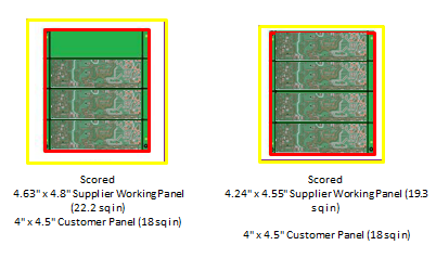
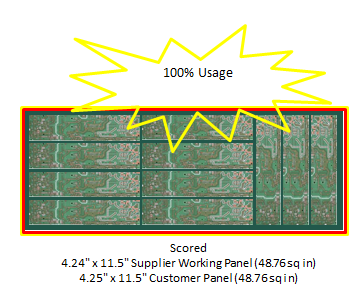
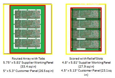
Panel Designer may provide options offering additional cost savings, with potentially very different geometries always striving for 100% material utilization / 0% waste.
Contact Us: info@sysargus.com
Learning Platform for Product Engineering professionals imparting guidance and sharing knowledge on Electronics System Design Best Practices.
Connect with us:-