Vias and Microvias
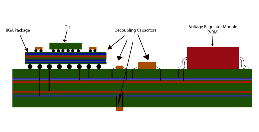
In a high-speed circuit, any metal on the PCB should be considered as part of that circuit. The trace lengths, the via size, and the via depth should be taken into account for high-speed circuit calculation. The designer should understand that the via drill size impacts the size of the via. The smaller the vias, the better will be the performance of the circuit. Once the designer decides on the vias sizes, the right placement of these vias close to their respective pads should be considered.
In high-speed design, the vias are placed close to the pad to avoid parasitic capacitance. Sometimes they are placed partially on the pad or entirely within the pad. These adjustments require DRC adjustments.
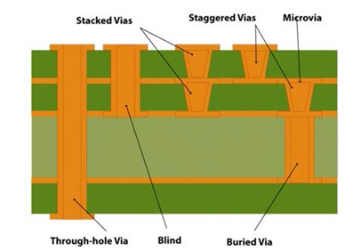
Depending on their functionality, there are different types of vias that are drilled into a PCB.
Through-hole vias
The hole penetrates from the top layer to the bottom layer. They can be either PTH or PNTH. For PTH, the connection is established from the top to the bottom layer.
Blind Vias
The hole penetrates from an exterior layer and ends at an interior layer. Here, the hole doesn’t penetrate through the entire board but connects the PCB’s exterior layers to at least one interior layer. Either the connection is from the top layer to a layer in the center or from the bottom layer to some layer in the interior region. The other end of the hole cannot be seen once the lamination is done. Hence, they are called blind vias.
Buried Vias
These vias are located in the interior region of the PCB. The buried vias have no paths to the outer layers. They connect the inner layers and stay hidden from sight. As per IPC standards, buried vias and blind vias must be 6 mils (150 micrometers) in diameter or less.
Microvias
The most commonly known vias are the microvias (µvias). During PCB manufacturing, micro vias are drilled by lasers and have a smaller diameter compared to the standard through-hole vias. Microvias are generally implemented in High-Density Interconnection (HDI) PCBs. The depth of micro via isn’t usually more than two layers deep since the plating of copper inside these small vias is a tedious task. The smaller the diameter of a via, the higher should be the throwing power of the plating bath to achieve electro-less copper plating.
Microvias can be classified into stacked vias and staggered vias based on their location in the PCB layers.
- Stacked vias are piled on top of one another in different layers.
- Staggered vias are scattered in the different layers. And they are more expensive.
- Additionally, there is another type of microvias called skipvias. Skipvias skip one layer, meaning, they pass through a layer making no electrical contact with that specific layer. The skipped layer will not form an electric connection with that via.
Microvias improve electrical characteristics and also allow miniaturization for higher functionality in less space. This, in turn, makes room for large pin-count chips that can be found in smartphones and other mobile devices.
Microvias reduce the layer count in printed circuit board designs and enable higher routing density. This eliminates the need for through-hole vias. The micro vias micro size and capabilities have successively increased processing power. The implementation of micro vias instead of through-holes can reduce the layer count of PCBs and also ease the BGA breakout.
Via-In-Pad
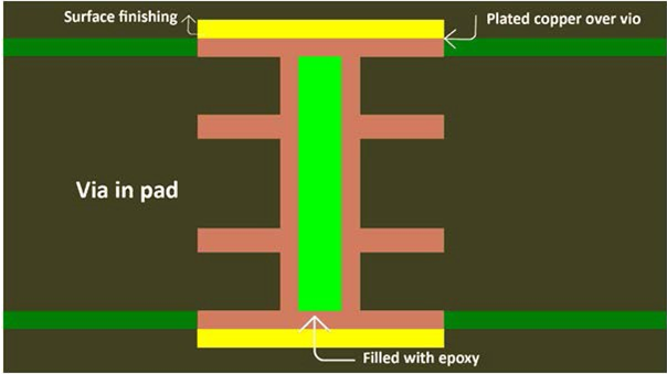
Implementation of via in pad or via in pad plated over (VIPPO) in your design
The increasing signal speed, board component density, and PCB thickness have led to the implementation of via-in-pad. The PCB design (CAD design) engineers implement VIPPO along with the conventional via structures in order to achieve profitability and signal integrity requirements.
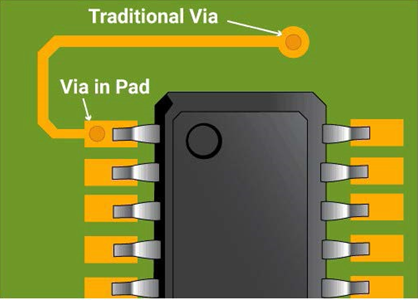
Via-In-Pad Vs. Traditional Via
What is Via-in-pad?
In traditional vias, the signal trace is routed away from the pad and then to the via. You can see this in the above diagram. This is done to avoid seepage of the solder paste into the via during the reflow process. In a via-in-pad, the drilled via is present right below a pad. To be precise, the via is placed within the pad of a surface mount component.
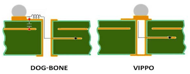
Traditional dog bone and VIPPO
First, the via is filled with non-conductive epoxy depending on the designer’s requirement. Later, this via is capped and plated to regain the land area. This technique shrinks the signal path lengths and as a result, eliminates the parasitic inductance and capacitance effect.
The via-in-pad accommodates smaller component pitch sizes and shrinks the PCB’s overall size. This technology is ideal for BGA footprint components.
To make things better, a back-drilling process is implemented along with the via-in-pad. The back drilling is performed to eliminate the signal reflections within the unused portion of the via. The unwanted via stub is drilled to remove any kind of signal reflection. This ensures signal integrity.
PCB Design Tips for Vias
Here are a few quick tips that you can consider while employing vias in your design:
- Use maximum micro via structures in your design.
- Stacked and staggered vias: Choose staggered instead of stacked vias since the stacked vias need to be filled and planarized. This process is time-consuming and expensive as well.
- Keep the aspect ratio minimum. This provides better electrical performance and signal integrity. Lower noise and crosstalk, and lower EMI/RFI.
- Implement smaller vias. This can help you build an efficient HDI PCB since the stray capacitance and inductance get reduced.
- Via-in-pads must be filled unless they reside in thermal pads.
- The pad matrix on which a BGA will be installed may include through vias and blind vias, but all of them must be filled and planarized, otherwise, solder joints will be compromised.
- Incorporate vias in the thermal pads under QFNs to help the solder flow through to conductive planes.
- The vias ensure a secure solder joint for the thermal pad and prevent the solder from floating the package during assembly, which could hamper forming good solder joints at the QFN contacts.
- An assembly shop can compensate for a lack of through vias in a thermal pad by adding a windowpane-shaped opening in the solder paste stencil above the pad, to relieve solder pooling and outgassing during assembly, but the fix is less effective than if vias were present.
- Check for minimum clearance of traces and vias from the routed/scored edges.
- Check the position of vias for BGA packages. Via-in-pad design requires filling.
- Dog-bone design: Separate each via from its pad with a predefined short trace covered with a solder mask. Ensure there is no mask clearance for the vias under BGA.
- The board documentation should include a drill file with tool codes and X-Y coordinates for all holes.
- The fab drawing should include a drill chart with hole symbols on the drawing and finished hole sizes along with via tolerances.
- The Gerber files should include via plugging holes if required.
- Controlled depth for blind and buried vias
Tolerance:
- Minimum outer layer annular ring: as per IPC standards
- Minimum inner layer annular ring: as per IPC standards
- Drill to plane clearance: 8 miles
- Diameter: ± 3 mils preferred
- Location: 1 mil
- Registration: 1 mil
- Via clearance of solder mask: 2.5 mils bigger than via pad size
- Encroachment of solder mask onto via: via size + 3 miles
- Anti-pad: 16 mils bigger than the hole size and plane relief preferred 8 mils
There may be requirements for fabricators to plug, fill, or tent vias on a PCB.
Via Design
The effects of via design are discussed in this section. The Via design depends on two parameters: the drill size and the pad size/annular ring. These parameters are recommended in IPC standards.
The drill size depends on the thickness of the board. In a power board requiring high currents, the drill size will depend on the current required per via.
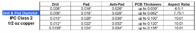
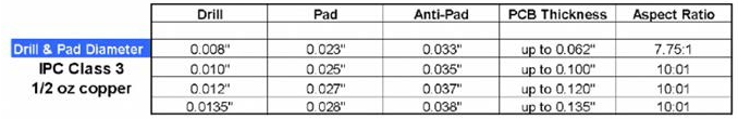
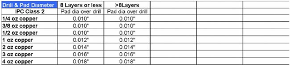
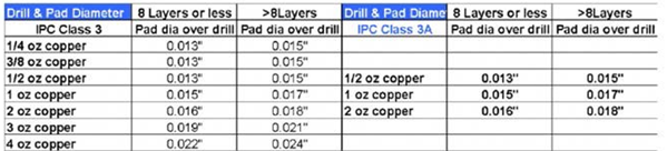
Class Type and Minimum Drill and Pad Requirements
The charts mentioned below show that for a class 2, 62 mil PCB, the recommended drill size is 8 mils with a pad size of 18 mils. For class 3, 62 mils PCB the recommended drill size is 8 mils and the pad size is 23 mils.
- Depending upon the Performance, the designs are classified as follows:
- Class-1: General electronic products
- Class-2: Dedicated service electronic products
- Class-3: High-reliability electronic products
- Drill values depend on the class of the design, fabrication technique, and PCB thickness.
Below given are the few values for Class-2 and Class-3 that should be followed.
Current carrying capacity of Vias
Vias are often used to tie power planes together and therefore it becomes necessary to know the current capacity of the via. To understand the current capacity of a via, it’s necessary to know the surface area of the via. The via forms a cylinder in the via drill hole. The length of the cylinder is the thickness of board ‘B’. The surface area of the cylinder formed via copper plating ‘p’ is given by p*D* B where D is the drill size or diameter of the drill hole. The thickness of the cylinder is equal to the plating thickness which is 0.8 mils. If the cylinder of the via is imaginarily cut along its length B and spread out, the via cylinder will be a trace of length B, thickness t=0.8 mils, and width p*D = 3.14 * via drill size. For 8 mils drill, the trace width would be 8*3.14 = 25.12. Using a standard trace current calculator with an ambient of 25 ⁰C and temperature rise of 5 degrees and since the via is not covered by solder its equivalent to an external trace. For an 8 mil drill the current capacity for 5 ⁰C temperature rise is 0.8 amps.
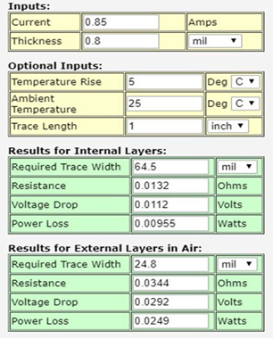
Table 1: Current calculator for trace width
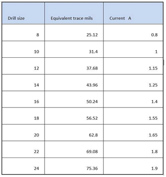
Table 2: Drill size and current capacity
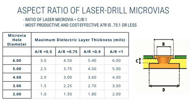
Microvias Design
Microvias are holes with diameters less than 6 mils. Practically speaking, vias possess an inductive and capacitive parasitic value. The smaller vias have lower capacitance whereas the short length, larger diameter vias have lower inductance. The inductive and capacitive parasitics will affect the high-speed signals.
The designer should use the upper layers for high-priority supplies. Placing high transient current supplies vertically closer to the device decreases the distance the currents need to propagate through the vias. Also, the ground planes should be adjacent to high transient current power planes to reduce inductance and couple the high-fre- quency noise.
The most important thing to consider while incorporating vias is the aspect ratio. The aspect ratio, via diameter to the dielectric thickness of the spanned layer, decides the reliability of a PCB.
Contact Us: info@sysargus.com
Learning Platform for Product Engineering professionals imparting guidance and sharing knowledge on Electronics System Design Best Practices.
Connect with us:-