Parts Placement Rules
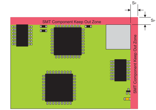
SMT Components to Edge
| Parameter | Standard | Advanced |
| Sp Perimeter Component Keep-Out Zone (no components or test pads) | 0.125 | Negotiable (requires special fixtures) |
On the solder (secondary) side of the PCB, the long edge of the PCB must have a clearance of 0.300″ on both sides. No SMT components should be placed there. Through-hole components that are to be hand-soldered or waved are okay.
The reason is that the Solder paste screen printing machine has hold-downs that attach to the secondary side of the board to prevent the board from moving during the paste printing process. These hold-downs may damage any component in this area as the paste is screened onto the PCB.
SMT Component-to-Component Spacing
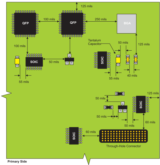
ALL DIMENSIONS IN THE TABLE ARE IN MILS
| To/From | Chip | Tantalum | SOIC | QFP/QFN | SOT23 | PLCC | BGA | CSP | DIP |
| Chip | 40 | 50 | 40 | 100 | 50 | 50 | 125 | 125 | 60 |
| Tantalum | 50 | 50 | 55 | 100 | 75 | 100 | 125 | 100 | 60 |
| SOIC | 40 | 55 | 50 | 100 | 50 | 100 | 125 | 125 | 60 |
| QFP/QFN | 100 | 100 | 100 | 100 | 100 | 100 | 250 | 250 | 100 |
| SOT23 | 50 | 75 | 50 | 100 | 35 | 100 | 125 | 125 | 60 |
| PLCC | 50 | 100 | 100 | 100 | 100 | 100 | 125 | 125 | 60 |
| BGA | 125 | 125 | 125 | 250 | 125 | 125 | 250 | 250 | 125 |
| CSP | 125 | 100 | 125 | 250 | 125 | 125 | 250 | 100 | 125 |
| DIP | 60 | 60 | 60 | 100 | 60 | 60 | 125 | 125 | 100 |
Sockets (for PLCC and DIP) and connectors should be away from BGA and CSP components to prevent solder joint cracking due to possible stress exerted during the second loading/removal of add-on cards or IC components.
For Advanced Option 0402 components can be 20 mils apart. and 0603 components can be 25 miles apart.
SMT Component-to-Component Spacing Examples
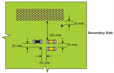
Distance is normally measured from pad edge to pad edge. However, in cases where the component’s body exceeds the pad dimensions (e.g. tantalum capacitors), the distance is measured from the body edge to the nearest feature (pad or component body).
Additional Secondary Side Restrictions
- Component height restrictions on the secondary side of the board should be less than 0.120″; the preferred height is less than 0.090″.
- Components taller than 0.100″ (e.g. tantalum capacitors or inductors) require 0.100″ clearance (land-to-land) in all directions to prevent solder defects (skips and opens).
- Minimum spacing of 0.025″ between SMT components (land-to-land) is required in both directions to prevent bridging.
- Minimum spacing of 0.025″ land-to-annular ring (via or through-hole component) is required to prevent bridging.
- Minimum spacing of 0.125″ land-to-annular ring required between all SMT components and DIP pins requiring selective wave solder fixture. Press-fit connectors are an exception and do not require this clearance on the secondary side.
- On the solder (secondary) side of the PCB, the long edge of the PCB must have a clearance of 0.300″ on both sides. No SMT components should be placed there. Through-hole components that are to be hand-soldered or waved are okay.
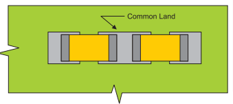
Only a single lead or termination should be placed on the land. Sharing a common land allows for one or both of the components to float during reflow. This causes unpredictable solder flow and part migration.
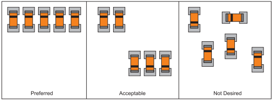
Component Orientation
All polarized SMT and through-hole components should be placed in the same orientation and in only one axis. This facilitates easier visual inspection. Where this is not practical, try to group components in the same orientation.
Placement Guideline for BGA’s and QFP/QFN’s
1. BGA and larger QFP devices (>100 leads) should not be placed in the center of the PCB. The maximum board warpage tends to be in the center of the PCB. The results can be open solder connections. For a standard 0.062″ PCB, this becomes a concern when the surface area exceeds 25 Square Inch.
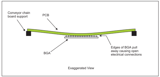
2. If BGA’s are on both sides of the board, it is not recommended that the BGA’s are positioned on top of each other. This method makes the rework of a BGA extremely difficult. In addition, this method makes X-ray inspection of the solder balls very difficult.
3. BGA’s should be placed on the top side of the PCB. This eliminates the possibility of open solder connections due to the weight of the part during the second pass reflow.
4. CBGAs and QFNs should not be on the same PCB. The reason is that CGBAs and QFNs require different amounts of solder. (CBGA components require more solder paste than QFN components.) Because of this, a step stencil or a separate solder stencil will need to be used for the CGBA to place the required amount of solder paste.
Should CBGA’s and QFN be placed on the same PCB, a minimum of 0.250″ clearance around the CGBA is required to accommodate the solder stencil.
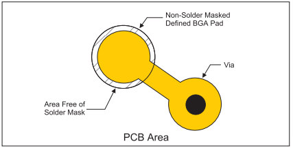
5. The traces that connect vias to BGA pads need to be masked off at a minimum to prevent solder from scavenging into the vias. The BGA pads are non-solder mask defined (i.e. solder mask opening is larger than the metal pad).
Contact Us: info@sysargus.com
Learning Platform for Product Engineering professionals imparting guidance and sharing knowledge on Electronics System Design Best Practices.
Connect with us:-