Need of Power Integrity Analysis and Its Approach in Board Design
Power Integrity
Power Integrity (PI) is Simply the assurance that power applied to circuit or device is appropriate for the desired performance of the circuit or device.
Power Integrity (PI) : Why ?
- IC’s used to have 1 power and 1 ground pin
- A Capacitor between the pins to provide local current
- Circuit Boards used to have one or two voltage rails.
- 3.3 and 5V.
- A plane for each.
- Today’s PCB Design :
- ICs with hundreds of grounds and power pins.Smaller Switching voltage means tighter tolerances on power supply voltagesMany voltage rails (more than 10).Less areas for power plane
- Smaller nm nodes with more transistors a smaller process leads to faster switching (High-frequency currents)
- Modern PCBs need power Integrity (PI) analysis
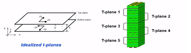
Power Integrity : Transmission Plane
- A Plane cavity that propagates electric and magnetic fields.
- Stores and propagates energy to IC power pins.
- Can intentionally carry other types of noise signals.
IR/DC Drop – Concept
- The equivalent electrical model of Power Delivery Network for DC Analysis
- ???? has DC Resistance
- Apply Ohm’s law to calculate voltage drop in ??DN
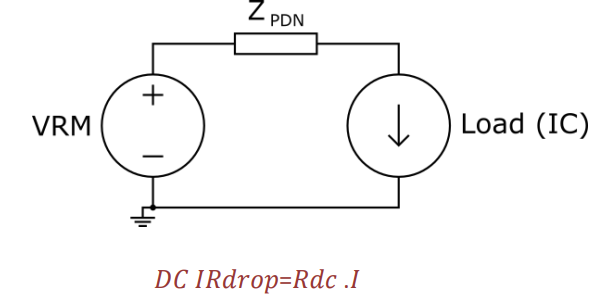
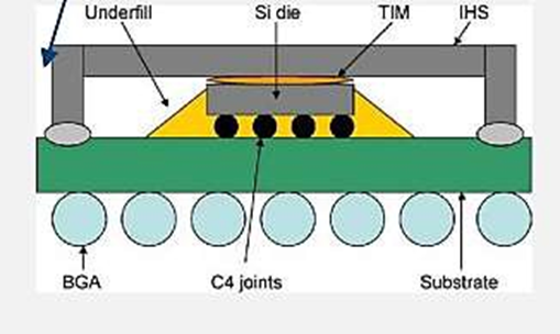
Note : The power distribution or delivery network (PDN) consists of all those interconnects from the voltage regulator module (VRM) to the pads on the chip and the metallization on the die that locally distribute power and return current.
DC Resistance
DC Resistance is determined by the geometry of the net and its material conductivity
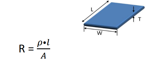
R = Resistance of Track
p = Resistivity of copper @ 20 0C (1.7241 ? −8 Ohm/m)
L = Length of track (1 cm = 1? −2 m)
A = Area in ?2 (For 35 um laminate, 1 mm track width = 35? −6 X 1? −3 ?2 )
R = 0. 0049 Ohms
Effect of Temperature
RT1 = ??0 + ??0 ⦁ Ct ⦁ (1 – ?0)
??0 = R at temp 0 (0. 0049 Ohms @ 20 Deg/C)
Ct = Temperature Coefficient of conductivity (for Cu +0.0039 / Deg K
(1 – ?0) = Temperature difference (∆ T = 65 Deg /C)
??0 ⦁ Ct ⦁ (1 – ?0 ) = Change in R due temperature difference
RT1 = 0.00614 Ohms
Current Density
- Current density is a measure of the density of an electric current. It is defined as a vector whose magnitude is the electric current per cross-sectional area. In SI unit, the current density is measured in amperes per square meter.
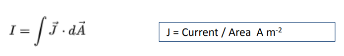
Where,
I = is current in the conductor
?= Is current density
D? = is the differential cross-sectional area vector
The current density (current per unit area) in materials with finite resistance is directly proportional to the electric field ?in the medium. The proportionality constant is called the conductivity of the material, whose value depends on the material concerned and, in general, is dependent on the temperature of the material.
Transmission Plane – In Practice
In Practice, Transmission planes have
- Void
- Antipodes
- Irregular shape
- Bottlenecks
Power Integrity: DC Drop Analysis Goals
- Goal of analysis is to improve the current design
- this is done by understanding how the current design performs
- Areas investigated during a DC Drop analysis are :
- Is there enough metal?
- What is the current through each part of the board?
- More current/Smaller piece = higher current density
- Whether or not design are met
- Maximum current density constraint
- maximum voltage drop constraint
- Maximum via current constraint
- After DC Drop analysis, possible changes made to the design are changes to:
- Planes Shapes
- Number of vias

Contact Us: info@sysargus.com
Learning Platform for Product Engineering professionals imparting guidance and sharing knowledge on Electronics System Design Best Practices.
Connect with us:-