High Speed PCB Design Guidelines – Minimize cross talk
Strategy: Minimize mutual capacitance and mutual inductance between adjacent signal return path pairs.
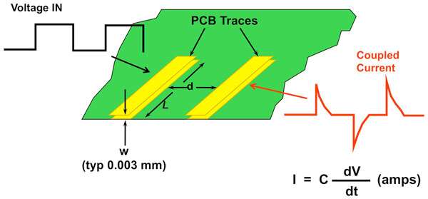
- For transmission lines, keep the spacing between adjacent signal paths at least twice the line width for microstrip or stripline.
- Minimize any discontinuities in the return path the signals might cross over.
- If you have to cross a gap in the return path, only use differential pairs. Never cross a gap with single ended signals routed close together.
- Capacitor is a not a low impedance interconnect structure. Its impedance will look like a 1-2 nH inductor above 10 MHz. It makes a poor “short” across a gap.
- For surface traces, keep the coupled lengths as short as possible and use as much solder mask as practical to minimize far end cross talk.
- If far end cross talk is a problem, add a laminate layer to the top of the surface traces to make them embedded microstrip.
- For long coupled lengths when far end cross talk may be a problem, route the traces in stripline.
- If you can’t keep the coupling length less than the saturation length, changing the coupling length will have no impact on the near end cross talk, so don’t worry about decreasing coupling length.
- Use the lowest dielectric constant laminate you can afford so the dielectric spacing to the return planes can be kept to a minimum for the same target characteristic impedance.
- In a tightly coupled microstrip bus, the deterministic jitter can be reduced by keeping the spacing at least as wide as twice the line width or routing timing sensitive lines in stripline.
- For isolations in excess of -60 dB, use stripline with guard traces.
- Guard traces can often make cross talk larger in surface traces unless the traces are very short.
- Always use a 2D field solver to evaluate whether you need to use a guard trace.
- If you do use a guard trace in stripline, make it as wide as will fit and use vias to short it to the return path and spaced at least 3 vias per rise time.
- Minimize ground bounce by making the return paths in any packages or connectors as short and as wide as possible.
- Use chip scale packages rather than larger packages.
- Minimize ground bounce in the power return path by bringing the power plane as close to the return plane as possible.
- Minimize ground bounce in the signal return paths by bringing the signal path as close to the return path as acceptable, consistent with matching the impedance of the system.
- Avoid using shared return paths in connectors and packages.
- When assigning leads in a package or connector, reserve the shortest leads for the ground paths and space the power and ground leads uniformly among the signal paths, or closest to those signal paths that will carry a lot of switching current.
- All no-connect leads or pins should be assigned as ground return connections.
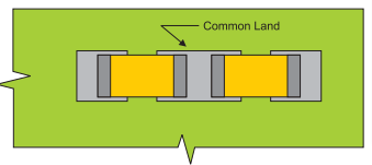
- Avoid using resistor SIPs unless there are separate return paths for each resistor.
- Check the Gerbers to verify antipads in via fields do not overlap and there is a well defined web between clearance holes in the power and ground planes.
- If a signal changes reference planes, the reference planes should be as closely spaces as you can afford. If you use a decoupling capacitor to minimize the impedance of the return path, its capacitance value is immaterial. Select it and design it in for lowest loop inductance.
- If many signal lines switch reference planes, space the signal path vias as far apart as possible, rather than clustering them all in the same location.
- If a signal switches reference layers, and they are the same voltage level, place a via between the return planes as close to the signal via as possible
Contact Us: info@sysargus.com
Learning Platform for Product Engineering professionals imparting guidance and sharing knowledge on Electronics System Design Best Practices.
Connect with us:-