Electronic Systems design for ESD Immunity
This article describes different ways to make your electronic equipment and electronic products immune to electrostatic discharge (ESD). Many of these techniques can also improve your system’s electromagnetic compatibility (EMC), electromagnetic interference (EMI), and overall robustness.
An ESD arc is an intense noise source with significant energy from 1MHz to 500MHz. This energy penetrates your system by every means possible, coupling into cables and printed circuit boards (PCBs), and may cause system upsets, lock-ups, or unwanted resets, as well as lost data and risk of permanent damage.
The key to effective immunity against ESD is to begin early in development, following conservative design practices and providing “wiggle room” in areas where you may need to tweak your design. ESD testing throughout development can also help you to find and fix weak spots as you go.
We defend against ESD by reducing the coupling into your system, and by making the system immune to transients through the use of any or all of the following methods:
- Plastic enclosures, air space, and insulation.
- Metal enclosures and shielding.
- Grounding and bonding.
- Power distribution, bypassing, and decoupling.
- PCB design and mounting.
- Cable design and routing.
- Filters and transient suppressors.
- Robust components.
- Robust circuit design.
- Watchdog timers.
- Software.
- ESD testing to find and fix weak spots.
Plastic Enclosures, Air Space and Insulation
Plastic enclosures, air space, and insulation prevent ESD arcs to a system (direct ESD):
- For >=20kV breakdown voltage, keep >=20mm air-path length between electronics and:
- Any points that users can touch- including ventilating/mounting holes and seams.
- Any ungrounded metal parts that users can touch- including controls, indicators, and fasteners.
- Any ungrounded metal parts that users can touch- including controls, indicators, and fasteners.
- Recess PCBs and cables in the enclosure, or use tongue-in-groove or shiplap seams.
- Cover unused connectors.
- Choose switches and controls with plastic shafts, or put plastic knobs (without metal setscrews) on metal shafts.
- Cover LEDs and indicators with insulating overlays, tape, caps, or light pipes
- Keep traces on membrane keyboards >=12mm inside the border, seal the circuitry layers or add a plastic bezel.
- Keep traces on tactile rubber keypads in tight, and extend the rubber top layer.
- Round corners and edges on heatsinks and metal parts that are close to ventilating/mounting holes and seams.
Metal Enclosures and Shielding
Metal enclosures and shielding intercept ESD arcs and their electric, magnetic, and electromagnetic fields, also protecting your system from external arcs (indirect ESD):
- Provide for >=20kV breakdown voltage between ungrounded enclosures and electronics, and >=1.5kV breakdown voltage (>=2.2mm air-path length) between grounded enclosures/shields and electronics.
- Design plastic enclosures to accommodate shields made of:
- Sheet metal
- Mylar/copper or Mylar/aluminum laminate
- Thermoformed metal mesh, metalized fiber mat, or metalized fabric
- Silver, copper, or nickel paint
- Electroless plating
- Zinc arc sprayVacuum metallization
- Highly-conductive fillers in the plastic (require special inserts to make contact)
- Aim for <=1 ohm/square resistance, using low resistivity metals (see Table 1).
- Choose compatible materials for shields, fasteners, and gaskets to minimize corrosion (see Table 1):
- EMFs within 0.75V (0.25V for salt-spray environments) for surfaces that will be in contact
- Surface area of the anodic part(s) is larger than the cathodic part(s)
- Overlap seams in shields by >=5 times the gap.
- Bond seams in shields at least every 20mm (0.8”) with welds, dimples, fasteners, finger stock, or conductive gaskets.
- Don’t nick, crack, or thin shields- make gentle bends and rounded corners.
- Make holes <=20mm (0.8”) diameter and slots <=20mm (0.8”) long; space openings apart by their largest dimension; use many small openings instead of one/a few big ones.
- If a control/indicator requires a larger opening, put a secondary shield between it and the electronics.
- For grounded equipment, connect shields to the chassis ground at the connector entry point.
- For ungrounded equipment, connect shields to the circuit common near switches and controls.
- Put a secondary shield parallel and close to susceptible electronics, connected to chassis ground/circuit common at the cable connection point.
- Put cable entry points near the center of conductive panels.
- Use Alodine, iridite, or chromate coatings on aluminum, and conductive chromate coatings on steel.
- Mask or scrape off anodizing and paint from seams, joints, and connectors.
- Don’t depend on hinges or screws for bonding. Force clean metal surfaces into direct contact. Put a ground plane next to a double-sided card, connected to the ground on the card at close intervals.
- Bond displays with a shielding coating to the enclosure, around the entire periphery.
Grounding and Bonding
Current from an ESD arc follows every available conductive path from the point of contact. Bonding minimizes the voltage drops along these current paths, while grounding drains off the charge:
- Keep the ESD current density and the current-path impedances as low as possible by using multipoint grounds where you want the current to flow, and single-point grounds where you don’t.
- Weld, braze sweat, or swage metal parts that don’t need to come apart.
- Bond metal pieces that must come apart by:
- Direct metal-to-metal contact between clean surfaces, held tightly together.
- Direct contact between metal surfaces with thin conductive coatings, held tightly together.
- Dimples or outside-star washers (to pierce paint/grease/insulating films) compressed between the metal surfaces.
- Protect bonds from moisture.
- Put multiple bonding straps or jumpers across hinges.
- Position bonding straps or jumpers away from PCBs and cables.
- Use solid bonding straps >=5mm wide where possible, braided bonding straps, and stranded bonding jumpers where you must.
- Choose compatible materials for bonding straps/jumpers and fasteners (see Rule 12).
- Make bonding straps short and wide, with width >= 1/5 the length and preferably >= 1/3 the length.
- Make gaskets >=5mm wide.
- Bring chassis ground to within 40mm (1.6”) of each cable entry point.
- Connect chassis ground to metal pieces of the enclosure, connector housings, switch housings, and control shafts (via grounding fingers or conductive bushings).
- Connect the grounds on all the boards inside an enclosure with multiple conductors.
- Connect chassis ground to circuit common with a ferrite bead.
- Encircle a membrane keyboard/rubber keypad with a wide chassis-ground guard ring, connected to the metal enclosure all around the periphery, or at least at all four corners- don’t connect this guard ring directly to circuit common.
Power Distribution, Bypassing, and Decoupling
Power distribution networks are prime targets for inductive coupling from ESD:
- Use multilayer PCBs with paired power/ground planes.
- Use tightly-interwoven power/ground grids on double-sided PCBs:
- Route power traces next to ground traces.
- Connect vertical and horizontal traces/infill with vias wherever possible.
- Keep power/ground grids <=60mm (2.4”) on a side, and preferably <=13mm (0.5”) on a side.
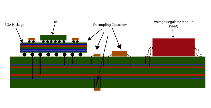
- Provide plenty of ceramic bypassing/decoupling capacitors on PCBs, close to their circuits/connectors.
- Tightly twist power wires and their returns together.
- Put a ferrite bead in each power line where it enters a PCB.
- Put a ceramic 1kV capacitor, metal-oxide varistor (MOV), or transient suppressor between each power pin in a connector and chassis ground.
PCB Design and Mounting
Intelligent PCB layout is our best weapon against ESD, and can incorporate most of the techniques described in this article:
- Design and protection circuits that you might need into your original layout (“wiggle room”). You can leave these components unpopulated or replaced by 0-ohm resistors if they aren’t needed:
- Put the protection circuit at the connector (preferred), or <=25mm (1”) from the receiver/driver.
- Position the components to minimize parasitic capacitance, mutual inductance, and the wiring common to the input and output of the protection circuit.
- Use short and wide traces (see Rule 35) to chassis ground/circuit common.
- Route signal and ground to the protection circuit, then to the receiver/driver.
- Make provisions for changing the grounding scheme, especially circuit common to chassis ground connections:
- Run chassis ground along PCB edges that have connectors to the outside world; use wide traces in all layers, tied together by vias about every 13mm (0.5”).
- Connect chassis ground to the connector housings and to any mounting holes on these edges. Use topside and bottom side pads without a solder mask put vias around the mounting holes, and don’t get solder on these pads during assembly. Screws with built-in Belleville washers connect the pads to tabs/metal standoffs on the chassis/shield.
- Make provisions for isolating/connecting other mounting holes to chassis ground- isolated pads with 0-ohm resistors to circuit common, choice of plastic or metal standoffs, etc.
- Separate circuit common/power from chassis ground by an identical 0.64mm (0.025”) wide moat in all layers.
- Connect circuit common to chassis ground by ground ties (1.27mm (0.050”) wide traces on the top and bottom layers) paralleled by pads for ferrite beads/capacitors at mounting holes and every 100mm (4”) along the moat.
- Put a circuit-common guard ring around the rest of the PCB:
- >=2.5mm (0.1”) wide in every layer you can, stitched together by vias about every 13mm (0.5”).
- Keep signal traces >=0.5mm (0.020”) inside this guard ring.
- Use multilayer PCBs with paired power/ground planes- they have 1-10% of the common-impedance and inductive coupling of equivalent double-sided PCBs:
- Put each signal layer next to a ground/power layer.
- Use a “submerged trace” scheme; the top and bottom layers have components and short traces, completely surrounded by ground; otherwise the signal/power wiring is on the inner layers, essentially encased in a Faraday cage.
- Put all connectors on one edge if you can.
- Put input/output circuits close to their connectors.
- Put ESD-susceptible circuits at the center of the PCB.
- Keep circuits compact.
- Put vias solid into power/ground planes.
- Make all signal traces as short as possible.
- Parallel signal traces that can get direct ESD hits, and signal traces >=300mm (12”) long, by ground traces.
- Keep resets, interrupts, and edge-triggered signals away from:
- The edges of the PCB.
- Unprotected input/output signals.
- Where permitted, fill in unused areas with the ground, with layers tied together by vias at least every 60mm (2.4”)- patches exceeding 25mm x 6mm (1” x 0.25”) should have at least two connections to the ground at opposite ends.
- If accidental slots in power/ground planes are longer than 8mm (0.3”), stitch the sides together with traces.
Cable Design and Routing
ESD can arc to the connectors on cables, while indirect ESD can couple into cables through induction or radiation:
- Keep cables short.
- Keep internal cables >=50mm (2.0”) from slots, seams, and bonding straps/jumpers, routed over continuous metal.
- Terminate cable shields to the outside of the metal enclosure/shield, preferably with 360-degree bonds- short and wide connections (see Rule 35) may suffice, but keep unshielded sections of the cable <= 40mm (1.6”) long.
- If you can’t reach the chassis ground, connect a cable shield to a circuit common with a 1-10nF 1kV capacitor or an anti-parallel pair of diodes.
- Choose compatible materials for mating connectors, connector backshells, and cable shields (see Rule 12).
- Minimize loop area inside cables by providing one ground wire per 1-5 signal wires; use S-G-S-S-G-S-S-G- S for flat cables.
- If a cable has spare wires:
- Connect them to the circuit common at both ends.
- Connect them to ground/power/signal wires at both ends.
- Clip them short, so they are completely enclosed by the shield
- Prefer coaxial cable, or twisted pair with at least 4 twists in the shortest wavelength of concern, to round cable or flat cable.
- Choose cable shields:
- – >=0.025mm (0.001”) thick.
- Prefer foil or foil-and-braid shields to braid shields, with metal-to-metal contact at the overlap.
- >=85% optical coverage for braid shields.
- Choose connectors with dimpled contacts between the mating connector shells, and between the connector shells and backshells.
- Fit ferrite sleeves on cables so that they encircle everything except the shield or shield drain wire(s).
Filters and Transient Suppressors
Filters and transient suppressors block ESD-induced voltages, and shunt ESD- induced currents elsewhere:
Determine the maximum capacitance you can put on the signal lines.
- Put filters on resets, interrupts, and edge-triggered signals.
- Put filters/transient suppressors on off-board receivers, and on off-board drivers for cables that can get direct ESD hits- including signals that go through optoisolators.
- Cascade low-pass filters (frequencies of f, 30*f, 1000*f, etc.) if needed. Filters are usually effective only up to 100-1000 times their design frequency.
- Follow power-line filters with high-frequency ESD filters.
- Configure protection circuits as:
- A blocking device.
- Shunt device(s) to chassis ground/circuit common.
- An L-network, with a blocking device and shunt device(s) to chassis ground/circuit common.
- A pi-network, with shunt device(s) to chassis ground, a blocking device, and shunt device(s) to circuit common.
- Connect blocking devices to ESD sources and low-impedance drivers/receivers:
- <=100k resistors for CMOS inputs.
- <=50-ohm resistors for bipolar inputs.
- Ferrite beads if low resistance is important. They provide 50-500 ohms impedance from 10- 1000MHz.
- Connect shunt devices to high-impedance drivers/receivers
- 100-1000pF capacitors to chassis ground.
- 10-100pF capacitors to circuit common.
- Clamps to chassis ground/circuit common.
- Crowbars to chassis ground/circuit common.
- Keep leads very short- 1nH/mm lead inductance slows down turn-on.
- Connectors are available with built-in capacitor arrays, ferrite sleeves, and MOV arrays.
- Limit transients to a safe voltage with clamps that turn on in <=1ns:
- Reverse-biased diodes to power and ground, with a 100-200nF bypass capacitor nearby.
- MOVs, multilayer varistors (MLVs), and multifunction capacitors (MFCs)- 0.5 ns turn on.
- Zener diodes and avalanche diodes- 0.05 ns turn on; can put a standard diode in series to reduce the capacitance.
- Limited by their maximum power dissipation.
- Short-out transients with crowbars that turn on in <=1ns- trigger level must exceed the maximum signal level, and hold current must exceed the maximum loop current.
- Choose components to withstand ESD voltages and currents:
- Thick-film and carbon composition resistors.
- Shunt capacitors that may take direct ESD hits should be rated
- >=1kV, or be large enough to absorb 2.3uC without exceeding their voltage rating if they aren’t protected by transient suppressors.
- Provide the same protective circuitry on all the signals going through a connector, to keep common-mode noise from becoming differential-mode noise- running all the wires through a common-mode choke works well.
| Metal | Electromotive Force (EMF), volts | Resistivity, nano ohm-meters |
| Magnesium | (anodic, corrodes) +2.37V | 42 |
| Magnesium alloys | ——— | 50 – 175 |
| Aluminum | +1.66V | 27 |
| Zinc | +0.76V | 60 |
| Galvanized steel | ——— | 100 – 197 |
| Aluminum alloys | ——— | 27 – 86 |
| Chromium | +0.74V | 132 |
| Cadmium | +0.40V | 73 |
| Mild steel | +0.44V | 100 – 197 |
| Iron | +0.44V | 101 |
| Tin-lead solder | ——— | 145 – 195 |
| Stainless steel | ——— | 560 – 780 |
| Lead | +0.13V | 206 |
| Tin | +0.14V | 126 |
| Nickel | +0.25V | 69 |
| Brass | ——— | 61 – 110 |
| Beryllium copper | ——— | 29 – 115 |
| Copper | -0.34V | 17 |
| Bronze | ——— | 91 – 212 |
| Monel | ——— | 510 – 614 |
| Silver solder | ——— | 22 – 172 |
| Titanium alloys | ——— | 482 – 1700 |
| Silver | -0.80V | 16 |
| Titanium | +1.63V | 540 |
| Gold | -1.50V(cathodic, passive) | 22 |
Table 1: Galvanic Series (in order of decreasing EMF)
| Technology | ESD Damage Threshold (Volts) |
| MOSFET’s | 10 – 200V |
| Recording Heads | 10 – 800V |
| VMOS | 30 – 1800V |
| NMOS | 60 – 500V |
| GaAsFET’s | 60 – 2000V |
| EPROMs | 100 – 500V |
| Laser Diodes | 100 – 1700V |
| JFETs | 140 – 7000V |
| SAW devices | 150 – 500V |
| CMOS | 150 – 3000V |
| Op Amps | 190 – 2500V |
| PIN Diodes | 200 – 1000V |
| DRAMs | 200 – 3000V |
| Schottky Diodes | 300 – 2500V |
| Film Resistors | 300 – 3000V |
| Bipolar Transistors | 300 – 7000V |
| SCRs | 500 – 1000V |
| ECL | 500 – 2000V |
| Schottky TTL | 500 – 2500V |
Table 2: Immunity to ESD Damage
Electronic engineers, PCB layout folks, mechanical engineers, and programmers must all cooperate to develop equipment and products with good ESD immunity. This is much easier when ESD immunity is considered throughout the design process, instead of treated as an afterthought.
Contact Us: info@sysargus.com
Learning Platform for Product Engineering professionals imparting guidance and sharing knowledge on Electronics System Design Best Practices.
Connect with us:-