High Speed PCB Design Guidelines – Minimize EMI
Strategy: Reduce the voltage that drives common currents, increase the impedance of the common current paths, shield and filter as a band aide.
- Reduce ground bounce by providing a low impedance, continuous return path under all signals, especially surface traces.
- Keep all traces at least 5 line widths from the edge of the board.
- Route traces in stripline when possible.
- Place the highest speed/highest current components as far from the I/O connections as possible.
- Place the decoupling capacitors in proximity to the chips to minimize the spread of high frequency current components in the planes. Don’t fool yourself into thinking capacitors provide low impedance above about 100 MHz.
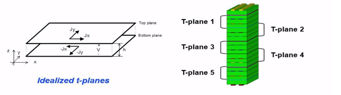
- Keep power and ground planes on adjacent layers as close together as possible.
- Use as many power and ground plane pairs as you can afford.
- When using multiple power and ground plane pairs, recess the power planes and stitch shorting vias between the ground planes along the edges.
- Use ground planes as surface layers, where possible.
- Know the resonant frequency of all packages and change the package geometry if there is an overlap with a clock harmonic.
- Avoid signals switching different voltage reference planes in a package. This will drive package resonances.
- Add ferrite filter sheets to the top of packages if they might have a resonance.
- Minimize any asymmetries between the lines in each differential pair.
- Use a common signal choke filter on all differential pair connections that leave the board.
- Use a common signal choke filter around the outside of all peripheral cables.
- Filter all external I/O lines to use the longest signal rise time that is tolerable for the timing budget.
- Use spread spectrum clock generator to spread the first harmonic over a wider frequency range and decrease the radiated energy within the bandwidth of the FCC test.
- When connecting shielded cables, try to keep the shield as an extension of the enclosure.
- Minimize the inductance of the shielded cable connections to the enclosure. Use a coaxial connection right to the end of the cable and connecting to the enclosure.
- Never use a pigtail connection between the cable shield and the chassis.
- Equipment bays should not penetrate the integrity of the enclosure.
- Only interconnects need to break the enclosure integrity.
- Keep apertures small diameter, significantly smaller than a wavelength of the lowest frequency radiation that might leak. More smaller holes are better than fewer large holes.
- The most expensive rule is the one that delays the product ship date.
Contact Us: info@sysargus.com
Learning Platform for Product Engineering professionals imparting guidance and sharing knowledge on Electronics System Design Best Practices.
Connect with us:-