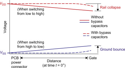
Minimize Rail Collapse
High Speed PCB Design Guidelines – Minimize Rail Collapse Strategy: Minimize the impedance of the power distribution network. Contact Us: info@sysargus.com Learning Platform for […]
High Speed PCB Design Guidelines – Minimize Rail Collapse Strategy: Minimize the impedance of the power distribution network. Contact Us: info@sysargus.com Learning Platform for […]
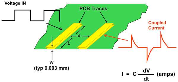
High Speed PCB Design Guidelines – Minimize cross talk Strategy: Minimize mutual capacitance and mutual inductance between adjacent signal return path pairs. […]
Ideally, all signals should use the Vss or gnd planes as their return planes so there is an option of placing return vias to reduce plane resonances.