Definition of ground bounce:
Ground bounce is a transient voltage generated between two different points on the same ground path, such as a package lead, a connector pin or different locations on the ground plane of a circuit board.
Any signal paths that use this ground path as part of their return will see the transient ground bounce voltage as noise. The ground bounce voltage noise will appear on all signal lines that share the common return path, whether there is a driven signal on the line or it happens to be pegged low.
If a daughter card is plugged into a connector and there is ground bounce voltage noise on the connector pins, the entire ground of the daughter card will “bounce” with the noise. If the shield of a cable is connected to a ground plane with ground bounce noise, the shield voltage can bounce with respect to the chassis. This can drive common currents in the shield and contribute to EMI.
Bounce Basics
FIGURE 1 illustrates a package that has five adjacent leads used as signals, while the sixth is used as a return for all five signals. When any of the signal lines switch, their return current will flow through the common return lead. A voltage will be generated across this lead and will be added to the signal path of the five signal leads. This ground bounce noise on the common lead will be a source of noise on each of the signal leads.
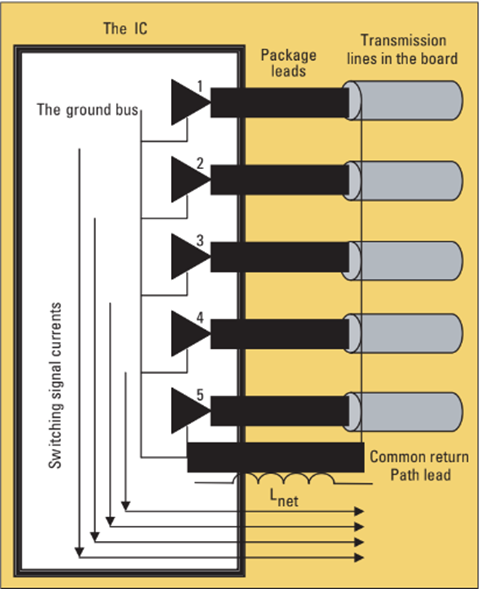
FIGURE 1.This leaded package features five signal leads and one return path lead. All switching currents use the same return path, and ground bounce is the voltage generated across the net inductance of that return path.
Figure 2 is an example of the simulated noise voltage that would appear on two of the signal leads when four signal leads are switching. One lead shown has signal while the other is pegged low. The voltage appearing on the quiet line is ground bounce.
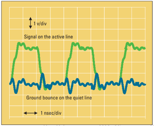
FIGURE 2. Ground bounce is shown on the fifth line, the “quiet” line, while the other four lines are switching.
Ground bounce is a form of crosstalk. In general, crosstalk is due to the capacitive and inductive coupling between two or more signal-return path conductors. When the mutual inductance dominates, we call this type of noise “switching noise,” as it is affected by the changing or switching currents through any mutual inductance between the coupled lines. The more lines that have mutual inductance between them and switch simultaneously, the larger the switching noise. This is why we usually call switching noise “simultaneous switching noise” (SSN) or “simultaneous switching output” (SSO) noise.
Ground bounce refers to the special case of switching noise when there is a shared return path, such as in a connector, a package, or when there is a gap in a return plane of a board and the return currents of multiple signal paths are forced to flow in the same part of the conductor.
Ground bounce voltage arises whenever a changing current flows through the total or net inductance of the return path. The amount of voltage depends on three parameters:
- The amount of current that switches, which is usually related to the number of signal paths that share the common return path and the current in each line.
- The rise time of the switching current.
- The net or total inductance of the return path.
The relative amount of ground bounce noise across a lead is roughly
Vgb/Va = n x Lnet/ (RT x Z0)
where
n = the number of signal lines switching simultaneously
Vgb = the ground bounce noise voltage
Va = the signal voltage on the active lines
Lnet = the net inductance of the return path
RT = the rise time of the active signals
Z0 = the characteristic impedance of the rest of the circuit.
For example, if there are four signal lines that share the same return lead in a package, and the rise time of the signal is 0.5nsec, with a 50Ω impedance environment and a total inductance for the return or ground lead of 2 nH, when any signal line makes up the rest of the loop.
In this typical case the relative ground bounce voltage would be 4 x 2/(0.5 x 50) = 32%. This much noise will exceed any noise budget and be a real problem.
Reducing Ground Bounce
Ground bounce voltage can be a serious problem in high-speed digital systems. As rise times decrease and bus widths increase, ground bounce becomes a greater problem. However, if we understand the origin of the problem, a few guidelines can help us keep ground bounce below the danger level and minimize it early in the design phase.
As with all signal integrity effects, the general strategy to reduce ground bounce to acceptable levels is to
(a) understand the physical origin of the effect
(b) adjust what you can and
(c) model and simulate the effect in order to balance the cost/performance trade-offs.
Unfortunately, most features in a design that reduce ground bounce also increase product cost. This is why it is so important to be able to model and simulate the effects of ground bounce. System design is all about designing for acceptable performance at the lowest cost. From the analysis above, following design guidelines can be followed to minimize ground bounce:
Reduce the number of signals sharing the same return path.
In leaded packages and connectors, there will often be situations where many signals use the same return pins or leads. In many connectors, there are three to five signals per return path. The ground bounce voltage across the return pin will be the sum of the noise from each signal line switching.
To minimize ground bounce, each signal line should have its own return pin in a connector or lead in a package. Of course, this means more pins are required for the return. This will increase the cost of the connector or package. The best case occurs when each signal has its own return pin. This is effectively what happens when all signals are routed as differential signals.
Increase the rise time of the signals
Since the voltage generated on the common ground lead is related to how fast the current changes, if you can increase the rise time of the current, the voltage noise will decrease. Use as long a rise time as practical. Unfortunately, rarely do we have the luxury of slowing down an edge and increasing the rise and fall times. When we try to do this, timing margins are affected, and meeting timing budgets is often as hard as meeting noise budgets.
In general, all signal integrity problems will increase with decreasing rise time. Never use a shorter rise time than you absolutely have to. With each reduction in transistor channel length, or die shrink, the rise time of the output drivers will get shorter. Always be aware of the output driver rise times and slow them down at the chip level using slew rate control when practical.
Reduce the net inductance of the return path
By far, the biggest bang for the buck in reducing ground bounce lies in reducing the total or net inductance of the return path.
It is the di/dt through this net inductance that generates the noise. Reduce the net inductance and ground bounce will also be reduced. But the design features that reduce the net inductance of the return path almost always cost more.
The total or net inductance of the return path is a measure of the total number of magnetic field line loops that encircle only the return conductor, per amp of current in the entire signal-return loop. The total inductance of the return path depends on the number of magnetic field line loops around the ground conductor that come from the current in the ground path, and the number of field line loops around the ground conductor that come from the signal path.
Since these two currents run in opposite directions, the total or net magnetic field line loops around just the ground conductor will be the difference in the number of field lines from the ground conductor and the signal conductor.
The golden rule in reducing the total inductance of the ground path is to decrease the number of field line loops coming from its own current and increase the number of field line loops coming from the signal path current. In package and connectors, this is accomplished with three design guidelines:
1. Use as short a trace for the shared return paths as possible. In TSOP and similar leaded packages, the shared return paths should be selected as the centre leads. Use chip-scale packages (CSPs) when possible; their leads are shorter than those of other leaded packages. In right-angle connector the pins in the shortest row should be used as return paths.
2. Use as wide a conductor as possible for the return path. In connectors a wide paddle is often used as the return path. In packages a plane can be used for the return path instead of a single lead. A two-layer BGA with a ground plane as the second layer will have less ground bounce than a two-layer BGA that has only ground traces. Multilayer BGAs with internal ground planes can have lower switching noise than leaded packages.
3. Bring the signal path as close as possible to the return path. In connectors and leaded packages, once the maximum number of return pins has been selected, assign the pins so the return leads are evenly distributed among the signal leads. The worst thing to do is put all the signals at one end and all the returns at the other end of the package or connector. Of course, there is a limit on how close to bring the signals and returns. The closer they are, the lower their impedance. If their impedance is lower than the impedance of the rest of the signal paths, reflection noise problems may arise.
Allow a continuous, wide return path in the ground plane.
Ground bounce can arise in the ground plane of a multilayer board when the return currents of the signal paths are forced together due to constrictions or gaps in the return path. The No. 1 way to reduce ground bounce in the return planes is to always provide a wide, continuous return path for each signal line.
Follow each signal path and look at the return path in the plane adjacent to it. The return path in the ground plane should have an unbroken path at least as wide as the signal line and preferably three times the width of the signal line. If there is a minor gap, route around the gap rather than across it.
Sometimes gaps are unintentional, as in the via field of a connector or package. To increase board yield, the fabricator may use a slightly larger aperture flash for the antipad holes in the ground planes. If over etched, these clearance holes might overlap, creating an unintentional gap.
Multiple signal lines passing through the via field will have return currents snaking around the edge of the gap in the return plane and overlapping, creating ground bounce. To avoid this source of ground bounce, make sure the web between clearance holes in the ground planes is as wide as you can afford, but at least as wide as the signal lines.
Power Distribution, EMI and Cost
Voltage on the ground return paths can also arise when the ground conductors are the return paths for the power distribution currents. Whether the ground bounce is created by the switching of signal currents or power currents, noise will be picked up by signal paths that share this common return path conductor.
Ground bounce created from the power distribution is reduced exactly the same way as when switching signal currents create it.
First, reduce the switching currents in the power distribution. One way to accomplish this is using differential signalling.
Another way is placing low-inductance decoupling capacitors as close as possible to the IC to localize the higher frequency components of the switching power and ground currents near the chip, and not through the net inductance of the ground planes.
use as wide and short a conductor for the ground paths as possible. Finally, bring the power path as close as possible to the ground path.
The optimum power distribution system designed for lowest ground bounce uses wide power and ground planes on adjacent layers with as thin a dielectric spacing between as you can afford.
Ground bounce can be a large source of crosstalk between signal paths that share the same common return paths. In addition, ground bounce voltages on the ground return paths of a board are often the dominant source of voltage that drives common currents on external cables and contributes to EMI.
Reducing ground bounce in the packages, the connectors and on the boards will reduce crosstalk and EMI. You can never eliminate ground bounce; all you can do is try to keep it below acceptable levels. But how do you know when you’re done? How do you know if it is low enough? The only way to know for sure is to “put in the numbers” with calculations or measurements. The only effective calculation tool is a 3D field solver that considers the precise current distributions in each conductor, especially the return planes. These are typically full wave field solvers, operating either in the time or frequency domain.
Contact Us: info@sysargus.com
Learning Platform for Product Engineering professionals imparting guidance and sharing knowledge on Electronics System Design Best Practices.
Connect with us:-