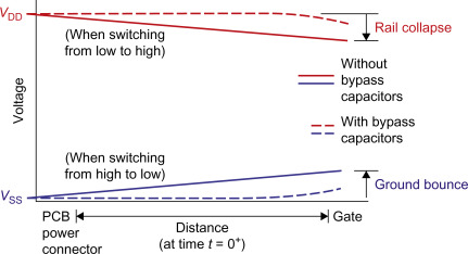
High Speed PCB Design Guidelines – Minimize Rail Collapse
Strategy: Minimize the impedance of the power distribution network.
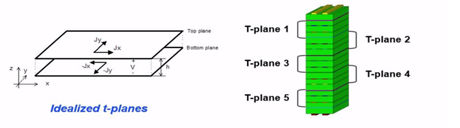
- Minimize the loop inductance between the power and ground paths.
- Allocate power and ground planes on adjacent layers with as thin a dielectric as you can afford.
- Get the lowest impedance between the planes by using as high a dielectric constant between the planes as you can afford consistent with the thinnest dielectric possible.
- Use as many power and ground plane pairs in parallel as you can afford.
- Route the same currents far apart and opposite currents close together.
- Place each power via as close as practical to a ground via. If you can’t get them at least within a pitch equal to their length, there will be no coupling and no value in proximity.
- Route the power and ground planes as close as possible to the surface where the decoupling capacitors are mounted.
- Use multiple vias to the same power or ground pad but keep the vias as far apart as possible.
- Use vias as large in diameter as practical when routing to power or ground planes.
- Use double bonding on power and ground pads to minimize the loop inductance of the wire bonds.
- Use as many power and ground connections from the chip as you can afford.
- Use as many power and ground connections from the package as you can afford.
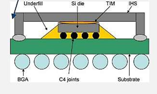
- Use chip attach methods that are as short as possible, such as flip chip rather than wire bond.
- Use package leads as short as possible, such as chip scale packages rather than QFP packages.
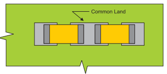
- Keep all surface traces between the pads of the decoupling capacitors and their vias as short and wide as possible.
- Use a total amount of bulk decoupling capacitance to take over from the regulator at low frequency.
- Use a total number of decoupling capacitors to reduce the equivalent inductance at high frequency.
- Use as small a body size decoupling capacitors as you can afford and minimize the length of all connections from the capacitor pads to the power and ground planes.
- Place as much decoupling capacitance as you can afford on the chip itself.
- Place as many low inductance decoupling capacitors as you can afford on the package.
- Use differential pairs for I/Os.
- The ONLY way of estimating the values and number of capacitors is using a simulation that includes the on-die capacitance and package lead inductance.
- If you don’t have any information about the package or chip, select capacitors and numbers to provide a flat impedance profile from 1 MHz to about 50 MHz.
Contact Us: info@sysargus.com
Learning Platform for Product Engineering professionals imparting guidance and sharing knowledge on Electronics System Design Best Practices.
Connect with us:-