


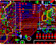
Our PCB Design environment uses best in industry tools like Mentor Graphics and Cadence for design capture, PCB layout and design analysis.We are customer centric and deliver high quality multi-layer high-speed PCB designs, taking into consideration of real-world manufacturing and test requirements. Our PCB design services includes:
Module 1: Schmatics Design Netlist generation DRC verification Module 2: Foot print creation Library maintenance IPC 7351 Slandered Module 3 Create a Layout Template. Start a PCB Layout by integrating with a schematic design. Define Board Geometry, Place parts, swap pins & gates and back annotate. Verify the Layout with on‐line and batch Design Rule Checking Utilize the Constraint Editor System (CES) to define layout and routing constraints Route, using both manual/interactive and automatic tools. Module 4: Generate Plane data Finalize the Silkscreen Generate Gerber Data.
About Us
Learning Platform for Product Engineering professionals imparting guidance and sharing knowledge on Electronics System Design Best Practices. more..
Contact Us
- Aura
- Email : info@sysargus.com
Copyright 2015 aura. All rights reserved.